Evaluation of the quality of commercial silicon carbide wafers by an optical non-destructive inspection technique
There is a great need for an in-line, high-speed and non-destructive inspection system capable of evaluating and analyzing the quality SiC wafers for SiC power devices. We have examined whether the laser-based optical non-destructive inspection system by KLA-Tencor meets these requirements. By optimizing the optical setup and improving the defect recognition and classification recipe, we have successfully mapped classified defects on a SiC wafer. Using this system, incoming inspection of purchased SiC wafers has been performed. The obtained inspection data show that micropipe density is sufficiently low in a device-grade wafer and, therefore, micropipes are not the main cause of device failure. The next challenges for a device-grade SiC wafer are reduction of epitaxial defects and relatively small defects classified as “particles”.
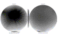
Fig. 1. Topographic image of 2-in 4H-SiC wafers from Vendor A and Vendor B.
Source: Journal of Crystal Growth
If you need more information about Evaluation of the quality of commercial silicon carbide wafers by an optical non-destructive inspection technique, please visit our website:https://www.powerwaywafer.com/, send us email at sales@powerwaywafer.com or powerwaymaterial@gmail.com.