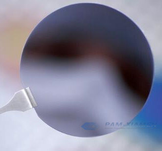
Xiamen Powerway(PAM-XIAMEN), a leading developer and manufacturer of compound semiconductor epitaxial wafers, provides 808nm AlGaInP/GaAs laser wafer. AlGaInP laser epitaxial wafers are high-quality semiconductor materials that can emit light in semiconductor lasers. After made on the laser chip, these materials are energized and can emit light. Then, the electrical signals are converted into optical signals. You can buy the following spec or custom-grown 808nm epitaxial wafer with AlGaInP material for laser:

1. AlGaInP / GaAs Epitaxial Structure for 808nm Laser Diode
| Layer | Material | X | Y Strain tolerance | PL | Thickness | Type | Level | |
| (ppm) | (nm) | (um) | (cm-3) | |||||
| 8 | GaAs | 0.1 | P | >2.00E19 | ||||
| 7 | GaIn(x)P | 0.49 | – | – | P | |||
| 6 | [Al(x)Ga]In(y)P | – | – | – | – | P | ||
| 5 | GaIn(x)P | – | +/-500 | – | U/D | |||
| 4 | GaAs(x)P | – | – | 798 | – | U/D | ||
| 3 | GaIn(x)P | 0.49 | – | – | U/D | |||
| 2 | [Al(x)Ga]In(y)P | – | – | – | – | N | ||
| 1 | GaAs | 0.5 | N | |||||
| 0 | GaAs substrate | N | ||||||
AlGaInP / GaAs LD Wafer Parameters:
| LD Wave Length (nm) | 808 |
| Size | 3” |
| Wafer PL or EL (nm) | 790+-5nm |
| PL Uniformity (6mm edge exclude) | +-1.5nm |
| XRD (for thick layers) | – |
| LD Slop Efficiency with AR + HR Coating (W/A) | >1.1 |
Source:PAM-XIAMEN
2. Applications and Development of Laser Epitaxial Wafer
Semiconductor lasers fabricated on GaAs laser diode wafers of PAM-XIAMEN can be widely used in laser pumping, advanced manufacturing, optical fiber communication, data storage, scientific research and medical beauty and other fields due to their small size, light weight, low threshold current, high electro-optical conversion efficiency, and can be pumped by injecting current. With the continued increase in consumer demand for high bandwidth, and gradually commercial 5G, the communication network will continue to upgrade, so the laser chip demand will continue to grow, thereby, the market of AlGaInP red laser diode wafer will goes up.
Depending on different application fields, high power is no longer the only indicator for evaluating the AlGaInP visible laser diode wafer:
For industrial processing, in addition to increasing the output power, the beam quality and brightness need to be further optimized;
When processing different laser materials, it is also necessary to consider the absorption band, and use lasers of different wavelengths for beam combination, which requires research and development of high-power lasers with different substrate material systems;
In order to further increase the combined beam power of laser wafer, it is necessary to further increase the combined beam spectral density and study new beam combining techniques;
For the application field of pumping single-mode fiber amplifier or output by coupling single-mode fiber, maintain single-mode performance, take convenience of single-mode fiber coupling as the primary goal, and increase the output power as much as possible on this basis;
In the fields of pumped atomic clocks, pumped laser gyroscopes, pumped alkali metal lasers, separated laser isotope, gas monitoring, optical fiber communications, satellite laser communications, etc., it is necessary to increase the InGaInP wafer of laser output power as much as possible while maintaining a single wavelength or narrow linewidth;
For application of AlGaInP LD wafer with high absorption efficiency in a certain absorption band, such as pump fiber lasers and solid-state lasers, it is necessary to increase the power of the useful band as much as possible to improve pump efficiency and reduce waste heat. It is necessary to adjust and optimize the output spectrum on the basis of increasing the output power.
3. FAQ of Laser Wafer
Q1:I plan to fabricate more than 10W LD , so can you advise a laser wafer that can we have 4mm cavity length?
A:Yes, you can use 4mm cavity length with a width of 200um for 10W LD.
Q2: What laser wafer I want is wavelength to be around 973nm , then PL wavelength might be 780nm
Can you adjust PL wavelength?
A: We suggest you use AlGaInP material, its PL wavelength should be 775-785nm.
Q3: With your experience , a laser wafer with cavity length for 4mm and emitter width for 185um are good enough for 10W LD chip?
A: Can not reach 10W, max.8W.
Q4: Can you suggest another Epi wafer that can reach 10W at 795nm?
A: If you want to reach 10W, the following structure should be used:
808nm LD structures
P+ GaAs P>5E19, d=0.15μm
P-AlGaAs and undoped AlGaAs d~1.5μm
Undoped AlGaInAs QW PL:975+-3nm
Undoped AlGaAs and N-AlGaAs, d~1.5μm
N GaAs buffer
N GaAs substrate N=(1-4)*1018d=350~625μm(100)15° off<111>A
Q5: Maximum achievable power with a standard laser diode bar with 19×100 micrometers emitters and 1 mm cavity length from 808nm and other wafers?
A:Bar output power of 808nm laser wafer: **W;
976nm: **W;
1064nm: **W.
Please contact victorchan@powerwaywafer.com for specific data.
Q6: Uniformity of QW PL across the laser wafer?
A: The uniformity of emission of 808nm laser epiwafer is less than 3 nm.
For more information, please contact us email at victorchan@powerwaywafer.com and powerwaymaterial@gmail.com.

