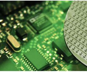
PAM-XIAMEN offer SiC wafer and Epitaxy: SiC wafer is the third generation wide bandgap semiconductor material with excellent performance. It has the advantages of wide bandgap, high thermal conductivity, high breakdown electric field, high intrinsic temperature, radiation resistance, good chemical stability and high electron saturation drift rate. SiC wafer has also great application prospects in aerospace, rail transit, photovoltaic power generation, power transmission, new energy vehicles and other fields, and will bring revolutionary changes to power electronics technology. Si face or C face is CMP as epi-ready grade, packed by nitrogen gas, each wafer is in one wafer container, under 100 clean class room.
Epi-ready SiC wafers has N type or Semi-insulating, its polytype are 4H or 6H in different quality grades, Micropipe Density (MPD): Free, <5/cm2, <10/cm2, <30/cm2,<100/cm2, and the available size is 2”,3”,4” and 6”.Regarding SiC Epitaxy, its Wafer to wafer thickness uniformity: 2% , and Wafer to wafer doping uniformity: 4%, available doping concentration are from undoped, E15,E16,E18,E18/cm3, n type and p type epi layer are both available, epi defects are below 20/cm2; All the substrate should be used production grade for epi growth;N-type epi layers <20 microns are preceded by n-type, E18 cm-3, 0.5 μm buffer layer; N-type epi layers≥20 microns are preceded by n-type, E18, 1-5 μm buffer layer; N-type doping is determined as an average value across the wafer (17 points) using Hg probe CV; Thickness is determined as an average value across the wafer (9 points) using FTIR.
-
SiC Wafer Substrate
The company has a complete SiC(silicon carbide) wafer substrate production line integrating crystal growth, crystal processing, wafer processing, polishing, cleaning and testing. Nowadays we supply commercial 4H and 6H SiC wafers with semi insulation and conductivity in on-axis or off-axis, available size:5x5mm2,10x10mm2, 2”,3”,4”, 6” and 8″, breaking through key technologies such as defect suppression, seed crystal processing and rapid growth, promoting basic research and development related to silicon carbide epitaxy, devices, etc.
-
SiC Epitaxy
We provide custom thin film (silicon carbide)SiC epitaxy on 6H or 4H substrates for the development of silicon carbide devices. SiC epi wafer is mainly used for Schottky diodes, metal-oxide semiconductor field-effect transistors, junction field effect -
SiC Wafer Reclaim
PAM-XIAMEN is able to offer the following SiC reclaim wafer services.
-
SIC Application
Due to SiC physical and electronic properties,Silicon Carbide based device are well suitable for short wavelength optoelectronic, high temperature, radiation resistant, and high-power/high-frequency electronic devices,compared with Si and GaAs device