Who We Are
Before 1990, we are stated owned condensed matter physics research center. In 1990, center launched Xiamen Powerway Advanced Material Co., Ltd (PAM-XIAMEN), now it is a leading manufacturer of compound semiconductor material in China.
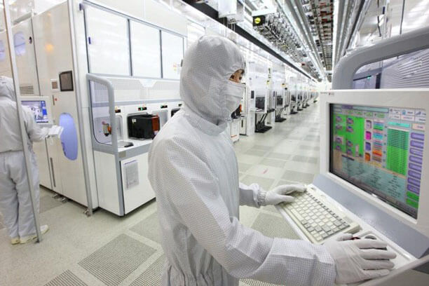
PAM-XIAMEN develops advanced crystal growth and epitaxy technologies, range from the first generation Germanium wafer, second generation Gallium Arsenide with substrate growth and epitaxy on III-V silicon doped n-type semiconductor materials based on Ga, Al, In, As and P grown by MBE or MOCVD, to the third generation: Silicon carbide and Gallium Nitride for LED and power device application.
Quality is our first priority. PAM-XIAMEN has been ISO9001:2008 certified and awarded honors from China General Administration of Quality Supervision, Inspection and Quarantine. We have owns and shares four modern factories, which can provide quite a big range of qualified products to meet different needs of our customers.
Welcome you to send enquiry to our sales team if you have any further question.Thank you!
Our History

2011
Commercial CdZnTe (CZT) wafer are on mass production,which is a new semiconductor, which enables to convert radiation to electron effectively, it is mainly used in infrared thin-film epitaxy substrate, X-ray and γ-ray detection, laser optical modulation, high-performance solar cells and other high-tech fields.

2009
PAM-XIAMEN has established the manufacturing technology for GaN epitaxy on Sapphire and freestanding GaN single crystal wafer substrate which is for UHB-LED and LD. Grown by hydride vapour phase epitaxy (HVPE) technology,Our GaN wafer has low defect density and less or free macro defect density.

2007
PAM-XIAMEN develops and manufactures compound semiconductor substrates-gallium arsenide crystal and wafer.We has used advanced crystal growth technology,vertical gradient freeze (VGF) and GaAs wafer processing technology,established a production line from crystal growth, cutting, grinding to polishing processing and built a 100-class clean room for wafer cleaning and packaging. Our GaAs wafer include 2~6 inch ingot/wafers for LED,LD and Microelectronics applications.Thanks to its mastery of molecular beam epitaxy technology (MBE) and Metal Organic Chemical Vapor Deposition(MOCVD),the company can offer world class epitaxial compound semiconductor wafers for microwaves and RF applications.

2004
PAM-XIAMEN has developed SiC crystal growth technology and SiC wafer processing technology, established a production line to manufacturer SiC substrate of polytype 4H and 6H in different quality grades for researcher and industry manufacturers,Which is applied in GaN epitaxy device,power devices, high-temperature device and optoelectronic Devices.As a professional company invested by the leading manufacturers from the fields of advanced and high-tech material research and state institutes and China’s Semiconductor Lab,we are devoted to continuously improve the quality of currently substates and develop large size substrates, as well as epitaxial technology.

2001
PAM-XIAMEN has established production line of semiconductor materials – Ge(Germanium) Single Crystals and Wafers.

1990
Xiamen Powerway Advanced Material Co.,Ltd(PAM-XIAMEN) founded. PAM-XIAMEN develops advanced crystal growth and epitaxy technologies, manufacturing processes, engineered substrates and semiconductor devices.

1990 -
We are stated owned condensed matter physics research center